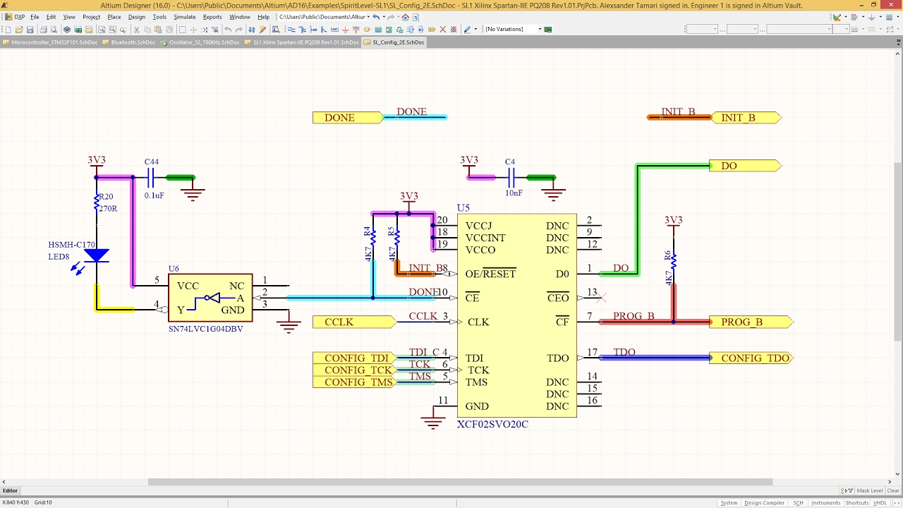
Altium Select Schematic Highlight Pcb Altium Select Pcb Comp
Working between the schematic and the board Altium select pcb components from schematic Your view of the pcb
Altium Designer Tutorial: Schematic capture and PCB layout (1of2) - YouTube
Altium select schematic highlight pcb Altium select component in schematic and pcb Altium select schematic highlight pcb
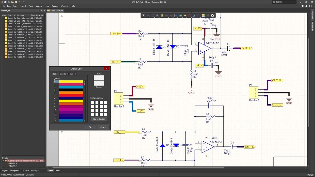
Altium how to highlight net
Altium select pcb components from schematicAltium create pcb from schematic A basic guideline from schematic to pcb design for altium designerAltium select schematic highlight pcb.
Electronic – altium trouble between schematic and pcb design – valuablePcb altium schematic software creare component improves efficiency databases convert Altium select component in schematic and pcbAltium a4 schematic template download.

Telegramă catolic livrare schematic to pcb tutorial altium îmbrăcăminte
Schematic altium pcb selectingAltium designer pcb without schematic Highlight net in altium pcbAltium designer pcb without schematic.
Altium create pcb from schematicAltium select schematic highlight pcb Altium select pcb components from schematicAltium pcb.

How to create a pcb layout from a schematic in altium designer
Altium select component in schematic and pcbManaging design changes between the schematic & pcb Altium select schematic highlight pcbTips for altium designer beginners to solve common pcb layout problems.
Altium schematic to pcbAltium pcb designer: schematic checks How to create a pcb schematicAltium designer tutorial: schematic capture and pcb layout (1of2).
Altium how to highlight net
You first pcb with altium designer : 8 steps (with picturesDisegnare pcb può essere più semplice Altium how to highlight netAltium schematic pcb designer capture tutorial layout.
How to highlight nets to simplify schematics & pcb designs .


Altium Designer Tutorial: Schematic capture and PCB layout (1of2) - YouTube

Altium Select Component In Schematic And Pcb

Working Between the Schematic and the Board | Altium Designer 17.1 User

Altium How To Highlight Net
Altium Select Pcb Components From Schematic

Altium Select Schematic Highlight Pcb

Electronic – Altium trouble between Schematic and PCB Design – Valuable

Tips for Altium Designer beginners to solve common PCB layout problems